Progressive die stamping, also known as transfer die, is a kind of cold stamping die that completes multiple stamping processes at different stations at the same time in one stroke of the press. This kind of mold has the characteristics of high precision, high efficiency and long life, so it is widely used in large-scale production.
In progressive die stamping molds, raw materials are continuously fed into various stations of the mold through a feeding device. Each station is responsible for a specific stamping process, such as punching, trimming, bending, drawing, etc. As the press travels, the raw material passes through the various stations in turn, and finally all the stamping processes are completed and the desired part or product is formed.
The advantages of progressive die stamping molds lie in their high efficiency and degree of automation. Since multiple processes can be completed at the same time in a single stroke, productivity can be greatly improved. In addition, the degree of automation of progressive die stamping molds is also high, which can reduce manual operations, reduce production costs, and improve product consistency and quality.
However, the design and manufacture of progressive die stamping is also more complex, requiring consideration of the coordination and coordination between the various stations, as well as the accuracy of the feeding device and the mold structure. Therefore, progressive die stamping are often used in large-scale production to give full play to their advantages of high efficiency and high quality.
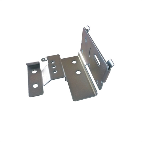
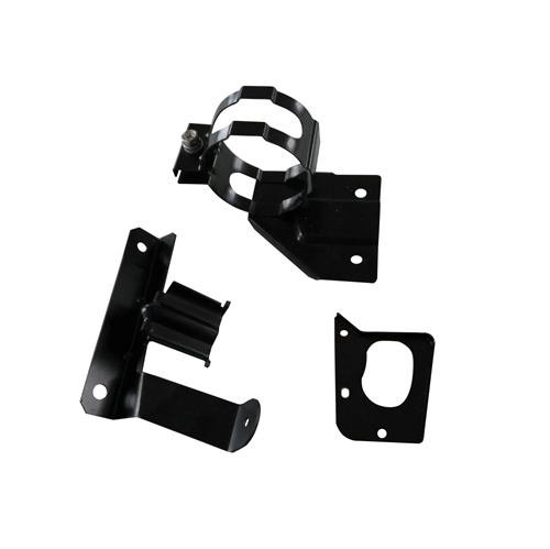
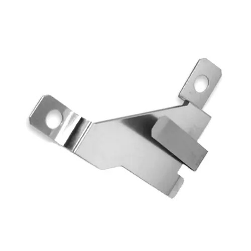
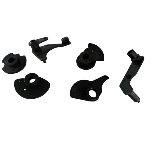
Progressive molds have a wide range of applications in the field of electronic product manufacturing. Electronic products usually have the characteristics of miniaturization, high precision, and complex structure, and progressive molds can adapt well to these needs. For example, in mobile phone manufacturing, progressive molds can be used to produce precision connectors, SIM card holders, and other components inside mobile phones. These components typically require high-precision dimensions and shapes, and progressive dies can ensure consistency and accuracy in each stamping process. For computer components, such as various interfaces on computer motherboards and fins on heat sinks, progressive molds can efficiently complete stamping processing to meet the needs of large-scale production.
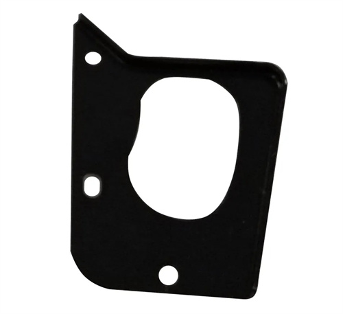
In consumer electronics products such as tablets, smartwatches, etc., their casings, buttons, and other components can also be formed by progressive stamping, achieving complex shapes while ensuring good surface quality. In addition, progressive molds can also be used to produce packaging shells for electronic components, such as chip packaging frames, providing assurance for the performance and reliability of electronic products.
In the rapidly evolving landscape of electronic product manufacturing, progressive die stamping has emerged as an indispensable technique for us. As we strive to meet the ever – increasing demands for high – quality, cost – effective, and precision – engineered electronic components, this manufacturing method offers a multitude of benefits that have transformed our production processes.
One of the primary advantages of progressive die stamping for electronic products is its ability to deliver unparalleled precision. Electronic components often require minute and exacting dimensions to ensure seamless integration into complex circuits. With progressive die stamping, we can fabricate components with tight tolerances, down to the micron level. For instance, when manufacturing connectors and leads for printed circuit boards, the advanced design and automation of progressive dies enable us to produce parts with consistent and accurate shapes, sizes, and surface finishes. This precision is crucial as even the slightest deviation can disrupt the electrical performance of an entire device, and we’ve seen a significant reduction in component failures and rework since adopting this method.
Speed is another key factor that makes progressive die stamping a game – changer in our electronic manufacturing operations. The continuous and automated nature of the process allows us to produce large quantities of components in a short period. Multiple operations, such as blanking, forming, and embossing, can be completed in a single pass through the die, eliminating the need for time – consuming manual transfers between different manufacturing stations. When we’re facing tight deadlines for high – volume orders of consumer electronics like smartphones or laptops, progressive die stamping enables us to ramp up production quickly and meet market demands without compromising on quality. We’ve been able to increase our output by as much as 70% compared to traditional stamping methods, giving us a competitive edge in the industry.
Cost – effectiveness is also a major benefit. Although the initial investment in designing and fabricating progressive dies for electronic components can be substantial, the long – term savings are significant. High – volume production spreads the cost of the die over a large number of parts, resulting in a lower cost per unit. Additionally, the reduced labor requirements due to automation translate into further savings. We no longer need to allocate as many resources to manual handling and repetitive tasks, which not only cuts down on labor costs but also minimizes the risk of human – induced errors. These cost savings allow us to offer more competitive prices to our customers while maintaining healthy profit margins.
Progressive die stamping also offers great design flexibility, which is essential in the ever – changing world of electronics. With the help of advanced computer – aided design (CAD) and computer – aided manufacturing (CAM) technologies, we can customize the die to produce a wide variety of electronic components with complex geometries. Whether it’s a specialized heat sink with intricate fins or a miniature metal housing for a sensor, we have the ability to modify the die design to meet specific product requirements. This flexibility enables us to adapt quickly to new product designs and technological advancements, ensuring that we can continue to supply innovative components to our customers.
Moreover, progressive die stamping contributes to improved material utilization. The efficient layout of the stamping process minimizes scrap generation. By carefully arranging the part shapes within the metal sheet, we can maximize the use of the raw material, reducing waste and cutting down on material costs. In an industry where every cost saving counts, this aspect of progressive die stamping is invaluable.
In conclusion, progressive die stamping has become an integral part of our electronic product manufacturing operations. Its precision, speed, cost – effectiveness, design flexibility, and material – saving capabilities have enabled us to produce high – quality electronic components that meet the stringent requirements of our customers. As the electronics industry continues to evolve, we’re confident that progressive die stamping will remain a key technology in our manufacturing arsenal, driving our success and helping us stay ahead of the competition.