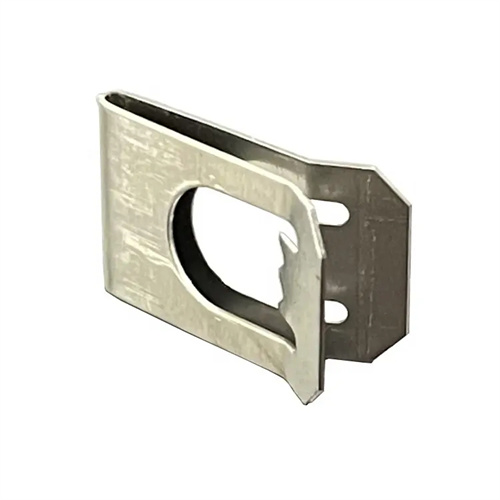
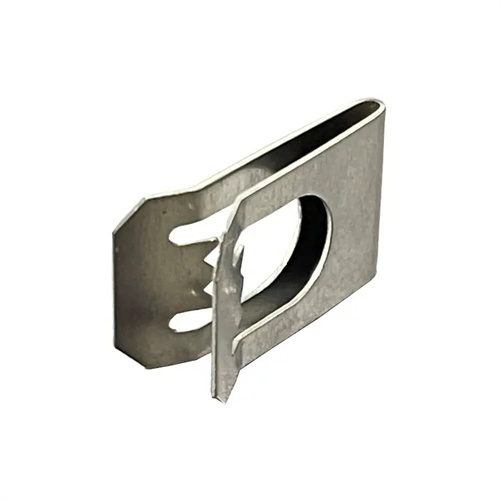
The high-precision stamping used for switches has a series of unique characteristics and advantages.
Firstly, it can ensure that the size and shape of switch components meet extremely high precision requirements. This means that key components such as the contact points and shrapnel of the switch can be accurately matched, ensuring the accuracy and reliability of switch operation. For example, in microswitches, high-precision stamped contacts can achieve extremely sensitive and stable contact.
Secondly, this process can produce switch components with complex shapes and fine structures. For example, the complex terminal structures of some multipole switches can be formed in one go through high-precision stamping, reducing subsequent processing steps.
Furthermore, high-precision stamping can ensure the smooth and even surface quality of switch components, reduce friction and wear, and extend the service life of switches.
In addition, it also has efficient production characteristics and can produce high-quality switch stamping parts on a large scale in a short period of time, meeting the large demand of the market.
In practical applications, high-precision stamping parts used for mobile phone button switches can provide comfortable pressing sensation and accurate response; In the field of industrial control, high-precision stamping ensures the stable performance of switches in harsh environments.
High precision stamping is widely used in the field of electronic products. This technology can meet the demand for high-precision and high-quality components in electronic products, providing strong support for the development of the electronic product industry.
Firstly, high-precision stamping is widely used in the manufacturing of electronic product casings such as mobile phones and tablets. These casings typically require a certain level of strength and exquisite appearance, and high-precision stamping technology can ensure the accuracy and quality of the casings while improving production efficiency. Through precise mold design and stamping processes, electronic product casings with complex shapes and precise dimensions can be manufactured to meet the aesthetic and usage needs of consumers.
Secondly, high-precision stamping is also used to manufacture internal components of electronic products. For example, key components such as electronic connectors and connectors have extremely high requirements for accuracy and reliability. High precision stamping technology can ensure the dimensional accuracy and shape consistency of these components, and improve the overall performance and stability of electronic products.

In addition, high-precision stamping is also applied in the manufacturing of electronic components, such as lead frames and shielding covers for integrated circuits. These parts need to have characteristics such as high precision, small shape, and thin material to meet the manufacturing requirements of integrated circuits. High precision stamping technology can achieve high-speed and precise stamping processing, ensuring the quality and performance of the lead frame.
With the continuous development of the electronic product market and technological progress, the application prospects of high-precision stamping in the field of electronic products will be even broader. In the future, high-precision stamping technology will continue to improve, providing more high-quality and high-precision components for the electronic product industry, and promoting the sustainable development of the entire industry.
In the realm of electrical and electronic manufacturing, we, as experts in custom high precision stamping for switches, understand the pivotal role our components play in ensuring the functionality, reliability, and longevity of various switch – based systems. Our work is a delicate balance of advanced engineering, meticulous craftsmanship, and a deep understanding of the unique requirements of switch components.
The essence of our custom high precision stamping for switches lies in achieving unparalleled accuracy. Switches are integral to countless devices, from consumer electronics to industrial control panels, and even the slightest dimensional variation can disrupt their performance. Using cutting – edge stamping technologies and state – of – the – art tooling, we are able to produce switch components with tolerances that are often within the micron range. For instance, when crafting contact blades for electrical switches, we ensure that their thickness, curvature, and surface flatness adhere precisely to the design specifications. This precision is crucial as it directly impacts the electrical conductivity, contact resistance, and overall switching performance of the device.

Customization is at the heart of our approach. We recognize that each switch design has its own set of requirements, whether it’s a specific operating force, a unique contact configuration, or a particular environmental resistance. Our team of experienced engineers collaborates closely with clients from the initial design phase, leveraging our in – depth knowledge of stamping processes and switch mechanics. Through detailed consultations, we gain a comprehensive understanding of their needs and translate those into tailored solutions. When a client in the automotive industry needed switches that could withstand extreme temperatures and vibrations, we developed custom – stamped components with enhanced durability and resilience, using specialized materials and innovative stamping techniques.
Quality control is a non – negotiable aspect of our production process. We have implemented a multi – tiered quality management system that begins with the sourcing of high – grade raw materials. Rigorous inspections are conducted to ensure that the materials meet our strict quality standards and are suitable for the demanding requirements of switch components. During the stamping process, we employ advanced monitoring systems that continuously track parameters such as stamping force, die temperature, and material feed rate. In – line inspection tools, including high – resolution cameras and automated measuring devices, are used to detect any potential defects in real – time. Additionally, our finished products undergo comprehensive functional and performance testing, simulating various operating conditions to guarantee their reliability.

Efficiency in production is another key strength we bring to the table. Our manufacturing facilities are equipped with high – speed progressive stamping presses that enable us to produce large volumes of switch components in a short period. The automated nature of our production lines not only increases productivity but also minimizes human error, ensuring consistent quality across all batches. We have also optimized our production workflows, reducing setup times and material waste through intelligent die design and layout planning. This allows us to offer competitive lead times without compromising on the quality of our products.
Innovation drives our continuous improvement. We are constantly researching and developing new materials, stamping techniques, and design concepts to enhance the performance and functionality of switch components. For example, we are exploring the use of advanced alloys with improved electrical and mechanical properties, as well as implementing novel stamping processes to achieve more complex geometries with higher precision. These efforts not only keep us at the forefront of the industry but also enable us to provide our clients with the latest and most advanced solutions for their switch – related needs.
In conclusion, as providers of custom high precision stamping for switches, we are dedicated to delivering components that combine precision, customization, quality, efficiency, and innovation. Our commitment to excellence ensures that the switch components we produce meet the highest standards of performance and reliability, contributing to the success of our clients’ products in the market.