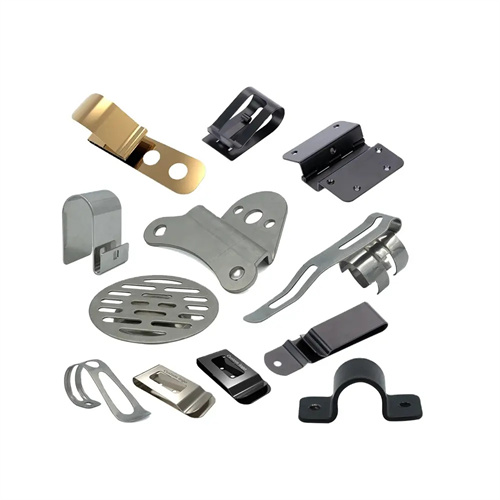
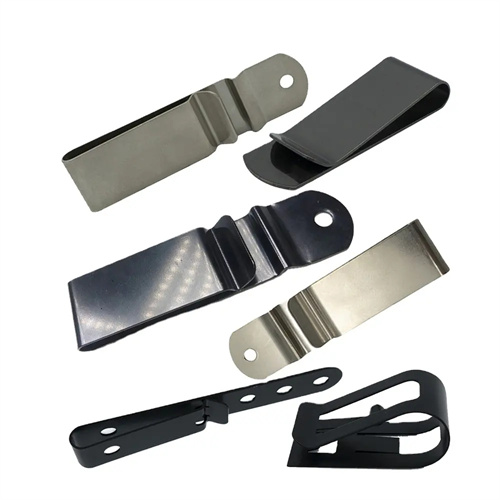
Unparalleled Precision in Electronics Spring Stamping
In the fast-paced world of electronics, precision is the cornerstone of our spring stamping services for contacts and connectors. We understand that even the slightest deviation in the dimensions of a spring contact or connector can disrupt the electrical performance of an entire electronic device. Whether it’s for a smartphone, laptop, or high-end server, our springs must meet exacting standards.
To achieve this unparalleled precision, we start with advanced design software. Our engineers use computer-aided design (CAD) tools to create highly detailed 3D models of spring contacts and connectors, taking into account factors such as electrical conductivity, mechanical durability, and space constraints within the device. During the manufacturing process, our state-of-the-art stamping presses, equipped with high-precision servo systems, can produce parts with tolerances as tight as ±0.01mm. Rigorous in-process inspections using optical comparators and coordinate measuring machines (CMMs) ensure that each spring stamping part meets our stringent quality requirements, making our products the go-to choice for leading electronics manufacturers.

Advanced Technology Driving Electronics Spring Stamping
Our commitment to excellence in spring stamping for electronics is powered by continuous investment in advanced technology. Our manufacturing facilities are equipped with the latest high-speed stamping presses that can handle a wide range of thin and delicate materials, such as phosphor bronze, beryllium copper, and stainless steel foils, which are commonly used in electronic contacts and connectors for their excellent electrical and mechanical properties.
We also leverage computer-aided manufacturing (CAM) systems to translate our detailed designs into precise production instructions for the stamping equipment. Additionally, simulation software plays a crucial role in predicting how the spring contacts and connectors will perform under various electrical and mechanical stresses. This allows us to optimize the design before production, reducing the risk of failures in the field. Furthermore, we are integrating artificial intelligence (AI) and machine learning algorithms into our production processes. These technologies help us monitor and control the stamping process in real-time, ensuring consistent quality and improving overall efficiency.

Streamlined Production Process in Electronics Spring Stamping
Our production process for spring stamping in the electronics sector is designed to balance speed, precision, and quality. It begins with the careful sourcing of high-quality raw materials from trusted suppliers. Each batch of metal foils undergoes strict inspection for thickness uniformity, surface finish, and material composition before entering the production line.
Once approved, the materials are fed into our automated stamping systems. Our progressive die stamping technology, with its multiple stations, enables the seamless transformation of flat metal foils into complex spring contact and connector shapes in a single pass. After stamping, the parts go through a series of post-processing steps, including plating for improved electrical conductivity and corrosion resistance, and heat treatment to enhance mechanical strength. Throughout the production process, our skilled technicians use in-line sensors and monitoring devices to detect any deviations from the set parameters. Any issues are immediately addressed, ensuring a smooth production flow and timely delivery of high-precision spring stamping parts for electronics.

Rigorous Quality Control in Electronics Spring Stamping
Quality control is the backbone of our spring stamping operations for electronics. We understand that in the highly competitive electronics market, the reliability of our contacts and connectors can make or break a product’s success. That’s why we have established a comprehensive quality management system that adheres to international standards, such as ISO 9001.
Our quality control team conducts multiple inspections at various stages of production. In addition to dimensional checks using advanced measuring instruments, we perform electrical tests to ensure proper conductivity and contact resistance of the spring contacts and connectors. We also subject the parts to environmental tests, including temperature and humidity cycling, to simulate real-world operating conditions. Any part that fails to meet our strict quality criteria is immediately rejected, and the root cause of the issue is investigated and resolved. This rigorous quality control process ensures that our spring stamping products for electronics are reliable, durable, and perform consistently under all circumstances.

Customized Solutions for Electronics Spring Stamping
We recognize that the electronics industry has diverse needs when it comes to spring contacts and connectors. That’s why we offer customized spring stamping solutions tailored to the specific requirements of our clients. Our team of experienced engineers and designers works closely with clients from the initial concept stage, understanding their product specifications, performance expectations, and budget constraints.
Using our advanced CAD/CAM capabilities, we can develop unique designs for spring contacts and connectors, whether it’s for a specialized application in the aerospace electronics sector or a high-volume consumer electronics product. We also offer a wide range of material options, surface treatments, and plating finishes to meet different functional and aesthetic requirements. Our flexibility in production volume, from small prototype runs to large-scale mass production, ensures that we can support clients at every stage of their product development. This commitment to customized solutions has earned us the trust and loyalty of numerous electronics companies worldwide.

Future Innovations in Electronics Spring Stamping
As we look towards the future, we are excited about the opportunities for innovation in spring stamping for electronics. The rapid advancement of technologies such as 5G, the Internet of Things (IoT), and artificial intelligence is driving the demand for smaller, more reliable, and high-performance electronic components. We are investing in research and development to explore new materials, such as advanced composites and nanomaterials, that can offer improved electrical and mechanical properties.
We also plan to further enhance our manufacturing capabilities by adopting more advanced automation and digitalization technologies. For example, we aim to implement smart manufacturing systems that can self-optimize the stamping process based on real-time data analysis. Additionally, we are exploring the use of additive manufacturing techniques for prototyping and small-batch production of complex spring contact and connector designs. By staying at the forefront of innovation, we are committed to providing cutting-edge spring stamping solutions for the ever-evolving electronics industry.